Dec 05, 2018 - Nixie MultiMeter, Part 17
Power
For this post, I will be focusing on the 3.3V digital and analog power supplies.
3.3V Power Supply
The first three steps when choosing a power supply are to establish basic requirements for voltage, current, and noise. For the 3.3V power supply, the voltage was chosen since it is a common voltage, and is compatible with the MSP430 (although the MSP430F6736 can run from voltages between 3.6 and 1.8V). The current requirement will be driven primarily by the worst-case current for each component which is powered from 3.3V. For many of these componets, the worst-case current is a combination of the maximum output current and the device’s internal worst-case current. The exact formulas can usually be found on the device’s datasheet.
| 3.3V Load | Worst-case Current |
|---|---|
| MSP430F6736 | 9.5mA, plus modules and outputs |
| LTC6078 (x2) | 160uA each, plus outputs |
| LMV358 | 340uA, plus outputs |
| Resistor drive | 100mA load on LMV358 |
| Virtual ground (200k) | 16.5uA |
| Reference Current | 80uA |
| Total | 110mA |
Clearly, the largest component of the 3.3V load comes from the drive circuit for resistance measurement. That’s also the part of the circuit where we’re most likely to see overloads, so that power supply should probably have significantly more capacity. Sizing the power supply at 200mA (almost 2x the required current) seems like a safe bet, and it shouldn’t be hard to find a switching (and maybe linear!) regulators that can do that.
Finally, the choice of power supply must consider noise, to help choose the type of regulator (switching or linear) and possibly choose several power supplies, if components need to have low-noise voltage supplies.
The MSP430F6736 datasheet strongly suggests powering the analog and digital supply pins from the same power supply. It seems like the obvious solution then is to use a single supply for all 3.3V loads, and add extra filtering on the supply for the high-precision part of the circuit. The amount of filtering required will be determined by the required output precision.
The ranges for both ADCs are +/- 14mV, over an 18-bit range, which comes out to about 107nV per bit. Any noise below that level will be undetectable by the ADC. The two components that will be affected by power supply noise will be the ADC within the MSP430, and the buffer op-amp.
Background on Decibels
I see decibels on a regular basis, but I rarely have to do math with them, so I’ll rehash the formulas here:
PSRR (dB) = 20 * log( power ripple / signal ripple )
Or, to go the other way:
power ripple / signal ripple = 10 ^ ( PSRR / 20 )
ADC Power Noise
The ADC has a power supply rejection ratio of -79dB or 1/8913; this means that any noise on the power supply will apear on the ADC reading, reduced by a factor of about 8913. Working backwards, the power supply ripple would have to be above 950uV ( 107nV * 8193 ) to affect the ADC reading.
This is a bit bogus, because the ADC only specifies a PSRR at 50Hz, but the average switching power supply operates between 100kHz and 2MHz. PSRR tends to be heavily frequency-dependent, with more coupling from power supply to ADC at higher frequencies, so this value is at best a lower bound, and at worst completely useless.
It may be more useful to look at the integration time of the ADC to determine how much power supply noise will affect the ADC readings. If the power supply noise is highly periodic with one or two major frequency components, and the ADC integration time is longer than several cycles, it seems likely that the power supply noise will average out before it appears on the ADC.
The ADC parameters that I selected (all the way back in part 6) were borrowed from TI’s reference design; they are a 2MHz modulator frequency and a 64x oversampling, for 19 bits of ADC resolution at 32k samples per second. Getting a switching power supply that runs several times faster than 32kHz should be easy. Given that the Sigma-Delta convertor works by sampling at high speed, in order to avoid aliasing the switching power supply frequency should not be close to any of the harmonics of the 2MHz sampling rate.
Aliasing occurs when two processes overlap at constant intervals; for example a 500Hz switching regulator frequency would be 1/4 of the 2MHz modulator frequency, and could cause 1 in every 4 ADC samples to land on a significant peak or trough of the power supply ripple, which would cause the power supply noise to be over-represented in the final ADC sample.
Typically, ADCs will have an analog low-pass filter at half the sample rate to filter out high-frequency noise; this filter would also help filter out power noise from other components, but it probably won’t help with noise induced within the ADC. For an ADC sampling rate of 32k samples per second, the Nyquist–Shannon sampling theorem states the the cutoff frequency should be set at half of the sampling rate; in this case that will be 16kHz.
LTC6078 Power Noise
The LTC6078 has a power supply rejection ratio of 97 dB, but it drops to zero around 4MHz:
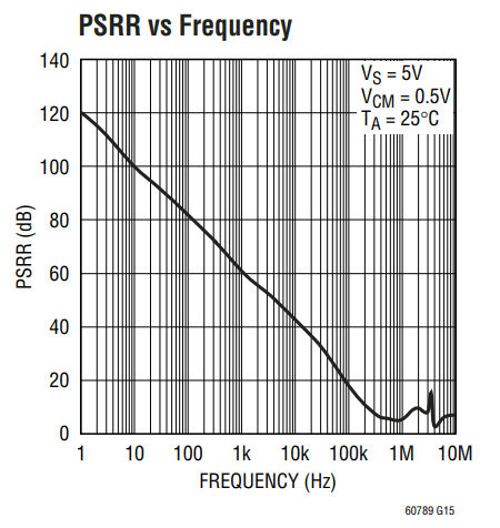
Since the ADC will have a low-pass filter on the input, we only need to worry about noise rejection in the LTC6078 up to the cutoff frequency of 16kHz.
At 16kHz and above, the PSRR is only about 25dB, or a reduction of about 17x between ripple on the power supply and ripple in the op-amp’s output. This means that a power supply ripple as small as about 1.7uV would be output as ripple of 100nV, and could appear in the ADC output.
Reducing the cutoff frequency to 10kHz would result in a PSRR of about 40dB, which is a 100x reduction in power supply ripple, and puts the maximum power supply ripple at 10uV.
Power supply ripple for switching supplies is typically in the 250kHz to 1MHz range, so either of these filters will probably be acceptable.
Power Filter
Based on the previous sections, the power supply and filters need to produce a 3.3V analog rail with no more than 10uV of ripple between a few hertz and the ADC sampling frequency of about 2MHz. This seems like a rather difficult target to hit, so I’m just going to try to create the best low-pass filter(s) for the power supply that I can, and see how close I can get.
The 3.3V supply will look something like this:
12V -> filter + regulation -> 3.3V -> filter -> 3.3V analog
Switching regulators can produce a significant amount of output noise, so using a switching regulator to produce the 3.3V rail, and then trying to remove all of the switching noise for the 3.3V analog supply doesn’t seem like it will work very well.
Instead, I should probably try to produce a 3.3V supply with the lowest ripple possible, and then use additional filtering between the 3.3V and 3.3V analog supplies to further suppress ripple and remove any ripple that might be introduced by the other components on the 3.3V rail.
From reading through The Art of Electronics, it looks like the best way to reduce any incoming ripple is with a combination of tranditional filtering and a circuit called a capacitance multiplier. After the filtering stages, a linear regulator can remove some of the remaining ripple and produce a regulated output voltage.
12V -> filter? -> capacitance multiplier -> linear regulator -> 3.3V -> filter -> 3.3V analog
(An interesting alternative is the LT1533 and described in Linear Tech App Note 70, but the IC is $10 and requires a separate transformer and inductors).
Linear Tech App Note 101 has some fantastic advice and characterization of the noise produced by switching regulators, and how to reduce or eliminate it. Mostly, the takeaway here is that switching regulators produce high-frequency transients (up to several hundred megahertz!) and that the parasitics in typical capacitors and regulators aren’t effective at blocking these frequencies, but that ferrite beads can be quite effective.
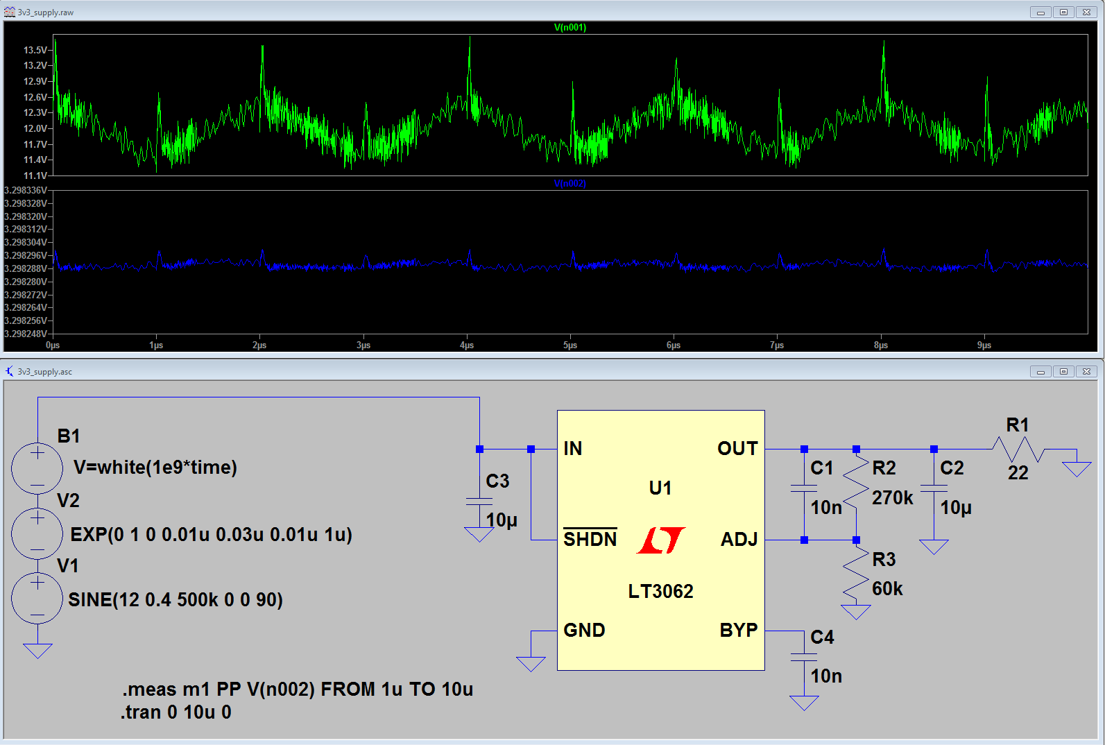
As as starting point, I’m going to try to create a noise simulation in LTSpice, and then simulate a circuit which can remove that noise (and probably substantially more). For a basic starting point, I’ve chosen a LT3062 since it is a linear regulator that can take the full 12V input voltage, has a model in LTSpice, and is relatively cheap. Unsurprisingly, it doesn’t have great power supply rejection at higher frequencies (10MHz), but at low frequencies it advertises an output ripple of 30uV!
As a starting point, I’ve created a simulation of the input (green, upper plot) and output (blue, lower plot) of the LT3062 (the adjustable version, hence the voltage-setting resistors). I’m simulating the ouput of a rather nasty switching power supply with a 0.4Vpp sine wave at 500kHz, a 1Vpp exponential with a fundamental frequency around 10MHz, and a healthy dose of white noise. I’m using a resitive load of 150mA, and the simulated regulator’s output is about 3.3V, with about 15uVpp of ripple. Not bad!
Adding a ferrite bead knocks down the random, high-frequency noise considerably, and adding a capacitance multiplier (completely untuned!) knocks down the remaining noise to a value that LTSpice doesn’t seem able to calculate correctly, but which appears to be less than 1uVpp. I’ll take it!
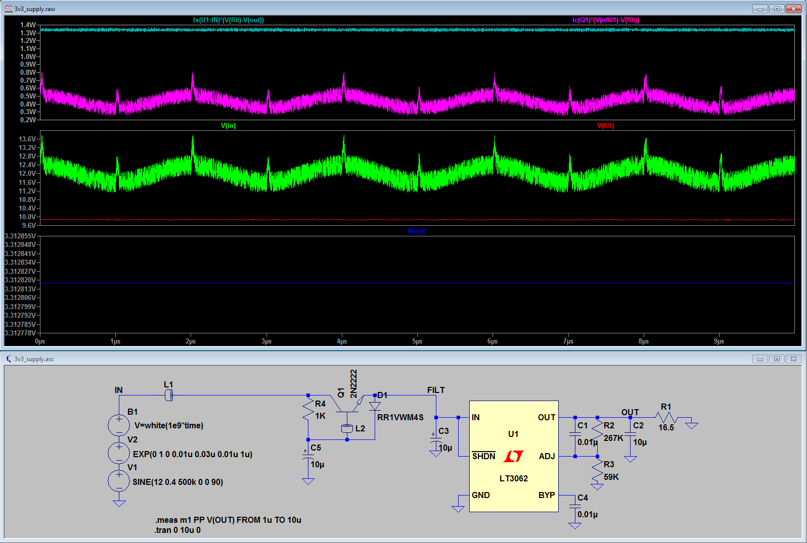
The only remaining consideration for this circuit is the power dissipation in the pass transistor and the regulator. Combined, all of the pass elements will need to drop 8.7V at up to 200mA, and dissipate the resulting 1.75W of heat. With the simulation at 200mA, the regulator needs to dissipate about 1.35W, and the pass transistor dissipates about 0.5W. I’d rater disspate that power in different part of the circuit, so I’ve added a resistor between the capacitance multiplier and the regulator. I’ve chosen the resitor value so that it drops about 5V and disspates about 1W at maximum current. At lower currents, it will have a lower voltage drop and disspate less current. At higher currents, it will limit the total current through the circuit.

For the final analog filter, it looks like the analog portion of the MSP430 can draw as much as 10mA. Each 24-bit ADC can draw a maximum of 1mA, not counting the current required to run the voltage reference. The 10-bit ADC can draw a maximum of 185uA, including the current required to run the voltage reference. Combined with 160uA for the LTC6078, the total current for the precision analog side of the circuit is about 11mA.
TI has a nice whitepaper on Filtering Techniques: Isolating Analog and Digital Power Supplies in TI’s PLL-Based CDC Devices, which describes common power filtering techniques and recommends a ferrite bead and ceramic capacitor filter between the digital and analog supplies. Given that this will only be filtering out noise induced by other components in the 3.3V circuit, this will probably be more than adequate.
Home