Mar 25, 2018 - Nixie MultiMeter, Part 13
Livestream from last week
For anyone who missed it on Twitter, I did another livestream a few weeks ago drawing up the HV5622 schematic symbol and footprint, and then including it in my schematic:
Miscellaneous Circuit Design Updates
3.3V to 12V Level Shifter
Between the microcontroller and HV5622 driver, I need a level shifter to increase the output voltage from 3.3V to 12V.
One of the most basic level shifters is an N-FET with a pull-up resistor on the output:
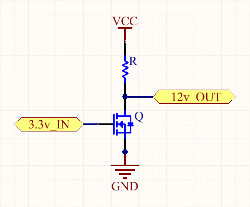
The resistor pulls the output up to approximately 12V, minus the voltage drop across the resistor from any loads on it.
When the N-FET turns on, it pulls the output low, driving current through the pull-up resistor and any loads on the output.
The biggest trick to designing this type of circuit is that the pull-up resistor needs to be chosen so that it pulls the output high enough that it is consistently read as a “1” by the load circuit (The Vih of the load). The tradeoff is that the smaller the pull-up resistor is, the more current it draws (and wastes) when the output is low.
This wasted power and the fact that the design depends on the load are both reasons why it isn’t used frequently.
For this particular level shifter, I have two design parameters from the HV5622 that are important here:
- The minimum input voltage is Vdd - 2V. (I’m going to leave this as Vdd - 2V since this 2V drop is what appears across the pull-up resistor)
- The maximum high-level input current is 1 uA. Since I have 2 HV5622’s, the total input current will be 2 uA.
This is a great use for Ohm’s law (V = I * R), and since we want to know the resistor value, we can rearrange to R = V / I. Plugging in the design paramters, I get: 2V / 2uA which is very conveniently equal to 1M Ohm. There’s probably some margin built into the input voltage, but with a design like this it’s better to plan for some additional margin, in this case 1V below Vdd would be half of the manufacturer’s suggested margin, so this seems like a reasonable design target. At 1V, the required resistor is still 500k Ohm.
When driving the output low, 12V will be applied across the 500k resistor, the resistor current will be 24uA and the power will be 288uA. This seems very reasonable.
3D View and Dual PCB
I put together a basic 3D model of the IN-17 nixie tubes and put them on a PCB in CircuitStudio, just to get a sense for how the physical design will work out.
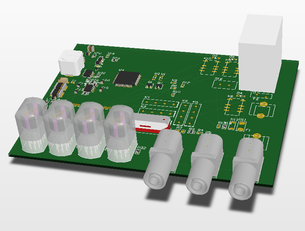
The obvious thing to note here is that the input jacks and the nixie tubes don’t face in the same direction.
Looks like I’ll need to put the nixie tubes onto a separate PCB for mounting. To keep the number of wires between both PCBs to a minimum, I’ll put the boost supply and both HV5622 chips on the nixie board. The only remaining wires running between the two boards will be the 5 control signals, 12V and GND, and maybe the HV enable signal.
Relay Driver FET
I’ve been contemplating driving the relays from the HV5622, but since I’m going to be putting both HV5622 chips on the nixie board, I’ll need to find another way to drive them. Since these relays need less than 100mA of driving current and already have protection diodes, almost any transistor will do here. I suspect I can use the same FET for the level shifter design and driving these relays.
Home