Jan 18, 2018 - Nixie MultiMeter, Part 5
Continuing on the previous post, I found a wonderful multimeter reference design from Texas Instruments, based on their MSP430 microcontroller line, that I’m going to review and will probably make the basis of my final design.
I’m starting by reading through the reference design document to get a better understanding of the design. The remainder of this post will be notes about the design and ideas for how I can adapt it.
Reference Design Review
It looks like this design does range switching using analog mux ICs instead of relays. This seems compact but may require some extra design steps if I want to use a broader range of input voltages. I will definitely need to make adjustments if I want to measure higher currents, since the analog mux passes the current during current measurement, and it almost certainly cannot handle the 10A range that I’m interested in.
Compared to previous designs, this design uses completely separate paths through the frontend, and separate ADCs for voltage and current measurements. This looks significnatly simpler, at the cost of an additional ADC, and allows simultaneous current and voltage measurements that can be used to compute power.
Instead of using dedicated circuitry for computing AC RMS values, this design uses a high-speed ADC and does the RMS calculation on the microcontroller.
Given sufficient processing power on the microcontroller, this could be used for some very intersting applications:
- Measuring the AC and DC components of the signal simultaneously, and alerting the user if they are in the wrong mode
- Correlating voltage and current measurements to compute the power factor of the load
This reference design use +/- 60mV inputs to both ADCs, which is apparently necessary so that the PGAs (programmable gain amplifier) and ADCs can operate with the same gain and filter settings, and therefore the same phase delay on both channels. The reference also refers to a 1V usable input range on the ADC. It sounds like it will be useful to review the MSP430’s PGA and ADC settings to select the right settings for my design.
The last 23 pages of the design document describe the calibration procedure and calibration results.
Schematic Review
There are a few things I didn’t learn from reviewing the reference design, such as how this design handles negative input voltages, so I’m going to review the schematic in detail in the hope that I can learn a bit more.
This design does not use an external precision voltage reference. Instead, it generates a reference voltage that is 1/2 VCC using an op-amp, and ties that to the V+ measurement lead and the positive side of a differential ADC input. The common measurement lead is then fed into a resistive voltage divider network and a unity gain amplifier, and the amplifier output goes into the negative side of the same differential ADC input.
Interestingly, this means that the common terminal of the range selection mux is also at 1/2 VCC. I’ll have to review the docs to be sure, but analog circuits tend to perform better when operated in this range, so this is a clever design choice.
There doesn’t seem to be any active input protection circuitry, but the Common measurement lead is connected to the rest of the circuit through a 10M resistor, which will limit the input current. The voltage divider is designed such that there is always a path from the common to V+ measurement lead, which prevents any of the internal circuitry from floating to a higher voltage. In the lowest range, about 90% of the input voltage is applied to the op-amp and mux inputs, through the 10M input resistor. I should evaluate the maximmum voltage range leakage currents and any protection on these inputs to determine if more protection circuitry is required or not.
Current measurement is done by placing a 0.5-ohm or 100-ohm resistance in the current path, and measuring the voltage drop across it through a unity-gain op-amp. The 200mA PTC fuse is rated to trip at about 460mA, which means that in the lower current range, the op-amp input could be as much as 46V! The PTC voltage rating is 24V, which isn’t enough to match the voltage range of the other inputs. Worse, the PTC is only subjected to its maximum voltage when it trips, which means that it could work correctly most of the time, and then fail if it trips and results in a very high voltage.
The PTC for current measurement is placed on the high side of the input, which is referenced to 1/2 VCC, but current measurement is performed on the low side of the PTC, which means that the I+ and I- terminals will be subjected to the voltage across the PTC when it trips, which will likely cause the op-amp, mux and ADC inputs to fail. Moving the PTC to the other input terminal would correct this.
A pair of back-to-back protection diodes in parallel with R13 would probably be the most effective method of protecting the mux and the op-amp from voltage transients, by conducting the transient and limiting the voltage applied across both components. I will need to choose this diode carefully so that the diode current at nominal operating voltage doesn’t interfere with operation, but that under extreme voltages the diode conducts strongly enough to limit the applied voltage. Increasing Vcc for the circuit may give me a little additional margin here too.
MSP430
I’ll probably come back to calibration later, but for now I’m going to swich over to reviewing the MSP430 datasheet and MSP430 user’s guide, looking specifically for details about the ADC section.
The datasheet appears to refer to the 24-bit Sigma-Delta analog converter that is used in the reference design as “SD24_B.” Page 71 of the datasheet has details about the ADC. For this design, I want to understand the maximum allowable voltage, since the protection circuitry must prevent voltages outside of this range, and I want to understand the full-scale input voltage, since this will determine the scaling factor needed between the inputs and the ADC to achieve the desired range.
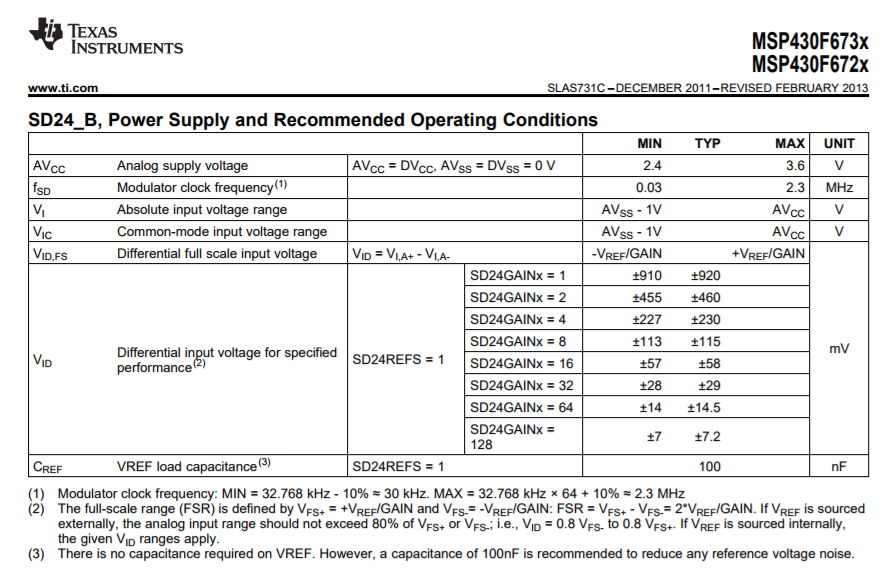
The maximum voltage on any of the ADC inputs is Vi and Vic, both of which range from Vss-1.0V to AVcc. The recommended differential voltage is Vid, and depends on the reference voltage. The reference design uses a gain setting of 16 with the internal voltage reference, which would correspond to a recommended differential voltage of +/- 57mV. Odd that this is slightly less than the +/- 60mV that is specified in the reference design, but it’s exactly equal to 80% of 1.2V / 16.
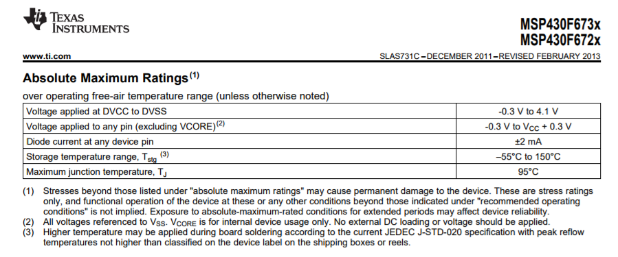
The Absolute Maximum Ratings section of any datasheet is always worth a read, and in this case it has a couple of useful bits of information. First, it lists the maximum voltage for any input pin, from -0.3V to Vcc + 0.3V. Second, it lists a “Diode current at any device pin” as +/- 2mA, which suggests that all of the input pins have protection diodes that can withstand 2mA of current. Since I know that the input pins are somewhat protected, I may not need as much protection circuitry elsewhere.
I had a quick skim through the MSP430 user’s guide, but I didn’t see any additional interesting information about the analog properties of the MSP430’s ADCs.
Home